For you we find customized solutions for non-contact optical inspection of wafers, probe cards, dies and microchip components. For this purpose, we offer systems for layer thickness measurement, contact inspection, electrical characterization, probe head positioning, sample manipulation and metrology of wafer microstructures in the nanometer range.
Technical features overview:
- Adaptation to the process: aperture, sample holder
- Safety concept and technology
- Customized design with frame, enclosure, integration into the fab
- Customer-specific development with 3D design, prototypes, series production
Custom Positioning Systems
 | travel 305 x 305 x 200 mm")
 | Stroke 200 x 200 mm")
 positioning system for wafer inspection / Raman spectroscopy up to 12\"/ panel (cleanroom ISO 4) | travel 400 x 400 mm")
 | travel XYZ 30 x 30 x 20 mm, RxRy 4°, Rz 360°")
 | Stroke 720 x 720 x 100 mm")


 | Stroke 720 x 720 x 100 mm")

 | rotary axis and linear stage")
")

Multi Axes Systems


 | Tripod, Rotary Stage, XY- Stage, Hexapod Alternative | Travel XYZ 30 x 30 x 20 mm, RxRy 4°, Rz 360°")


 | XY linear motor, profile rail | Phi belt, DC Motor | Travel 300 x 300 mm x 360°")
 | XY linear motor, profile rail | Z cross roller, ball screw drive | Phi belt, DC motor | Travel 450 x 350 x 16 mm x 45°")
 | XY linear motor, profile rail | Phi DC Motor | Travel 200 x 250 mm x 360°")
Standard Axes & Stages


Vacuum / Cleanroom


Ball & Lead Screw Drives


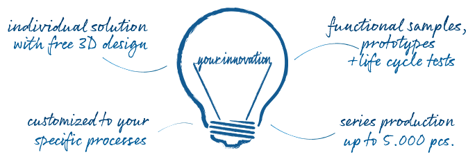
Individual customization and development of your Innovaiton
- Optimal positioning solution for your application with a fast and free 3D design
- Design of functional samples, prototypes up to series production
- Integrated development of your mechanics, electronics and software
- Series production of your innovation on > 3.900 m² production area
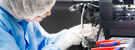
Cleanroom systems up to Class 2
On more than 100 m2 of cleanroom space, we exclusively manufacture high-precision and particle-free state-of-the-art technology for cleanroom systems up to ISO 14644-1 Class 2.
More on series development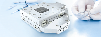
Vacuum standard axes up to 10-12
Our high-precision modular vacuum stages for linear, lifting, rotary and XYZ positioning have proven themselves over decades. They withstand the most extreme life tests with 24/7 operation.
Go to Vacuum Standard axes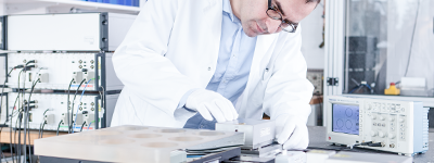
Individual life cycle tests
We implement your life cycle tests for you at our numerous universal test stands for various individual test scenarios in our measurement laboratories.
More about test and measurement
Katja Weißbach
Consulting
T +49 351 88585-64
E-Mail

Ronald Schulze
Consulting, Project Management & Engineering
T +49 351 88585-67
E-Mail

Francisco Samuel
Consulting &
Project Management
T +49 351 88585-85
E-Mail

Elger Matthes
Consulting, Concepts, Innovation & Engineering
T +49 351 88585-82
E-Mail